Tungsten and Tungsten Silicide Chemical Vapor Deposition
Applications
Tungsten (Wolfram for European types) is an extremely hard and refractory transition metal. W is fairly inert to wet chemical attack but readily etched in fluorine plasmas. It has several important applications in semiconductor fabrication.
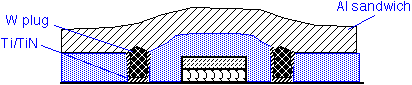
Deposition of pure W can be used to fill the holes that make contact to the transistor source and drain ("contact holes") and also to fill vias between successive layers of metal. This approach is known as a tungsten plug process. Tungsten is used because of the extraordinarily good conformality of CVD from WF6. It is necessary to provide an adhesion/barrier layer such as Ti/TiN, to protect the underlying Si from attack by fluorine and to ensure adhesion of W to the silicon dioxide. This approach appears to still be in use in (at least) 28 nm CMOS processes, using copper rather than aluminum as the lowest metal layer.
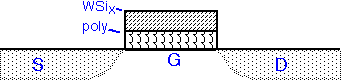
The silicide can be used on top of polysilicon gates to increase conductivity of the gate line and thus increase transistor speed. This approach was popular in DRAM fabrication, where the gate is also the word line for the circuit. WF6 and SiH4 can be used, but dichlorosilane (SiCl2H2) is more commonly employed as the silicon source, since it allows higher deposition temperatures and thus results in lower fluorine concentration in the deposited film. In modern processes silicide is simultaneously formed on the gate and S/D regions, often using tantalum or other metals instead of tungsten. Processes past about 40 nm often use replacement metal gates instead.
Deposition of W is almost always by CVD from tungsten hexafluoride, WF6. WF6 is a quite volatile liquid at room temperature; the vapor may be delivered directly delivered through a metering device (mass flow controller) from the reservoir. WF6 reacts readily with any moisture present to produce tungsten oxides and hydrofluoric acid, HF. It is imperative to avoid moisture in the plumbing: purged high quality stainless steel and metal seals are required. The liquid will produce copious HF vapor if exposed to air and thus must be considered quite hazardous; toxic monitoring and protective equipment are necessary. Dichlorosilane is a volatile liquid at room temperature, and will react readily with air to produce hydrochloric acid (HCl); thus, similar precautions in plumbing and handling are appropriate. We have discussed the issues associated with handling silane previously.
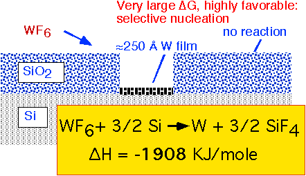
The direct exposure of a silicon substrate to WF6 at pressures of a few Torr results in the self-limiting formation of a thin layer of W metal. The reaction with silicon involves a large change in free enthalpy and is highly favored, whereas silicon dioxide is substantially inert to reaction with WF6. Thus, thin layers of W metal can be selectively grown on exposed silicon.
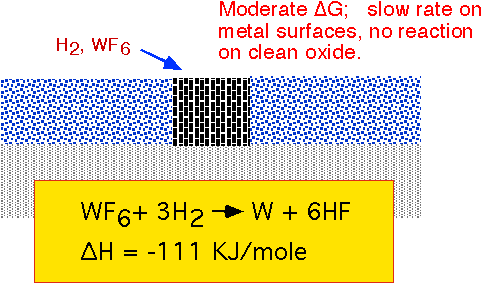
Reduction of WF6 by hydrogen can proceed readily on any metallic surface, but proceeds slowly or not at all on clean thermal silicon dioxide. This approach was examined in the 80's as the basis for selective growth of W in contact vias, but commercialization was extremely difficult due to sensitivity to trace moisture in the plumbing and reactor, and to damage to or contamination of the oxide surface by previous process steps. It was abandoned in favor of blanket deposition followed by etch back or removal by CMP (chemical mechanical polishing) in the 90's.
To get reasonable deposition rates from this reaction, fairly high pressures are required: 10-60 Torr. Typical temperatures are 300-500 °C.
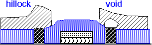
The use of tungsten in metal interconnects has important reliability implications. Tungsten atoms do not drift readily under the influence of electric currents (electromigration) or mechanical stress. However, they form a barrier for the movement of aluminum or copper atoms.
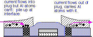
As a consequence, long aluminum runs connected at the ends with tungsten vias may fail preferentially at the vias under extended high current stress.
Copper is much more resilient than aluminum, but the lines are very tiny in modern processes, so electromigration failures can still be an issue.
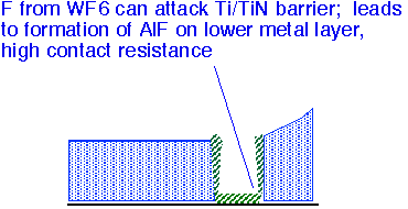
Fluorine from the WF6 precursor can also attack a TiN barrier layer and then etch the underlying Si layer. Poor conformality of sputtered TiN films can lead to especially thin films at the bottom corners of via holes; CVD TiN barriers can be useful to reduce vulnerability to attack.
Adhesion of CVD tungsten to sputtered Ti, TiN, TiW and related materials is excellent. Adhesion to CVD silicon dioxide is generally poor. When sputtered adhesion layers are employed, coverage at and under the wafer edge is generally poor, whereas CVD W readily deposits on all exposed surfaces. This excessive coverage results in W deposited directly on underlying oxides at the wafer edges; the W metal there readily spalls off as metal particles in cleaning baths or upon thermal cycling. Therefore, it is important to make provisions to exclude deposition of W on the wafer edge in design of W CVD reactors. A specialized wafer chuck design providing gas flow around the wafer edges is used for this purpose.
- - - - - - - - - - - - - - - - - - - -
Much of the development of WF6-based CVD was reported in a series of symposia "Tungsten and Other Refractory Metals for VLSI Applications" I through (at least) V, from about 1985 to 1990, sponsored by the Materials Research Society (MRS).
Some other specific references:
"Surface Chemistry of the WF6-based Chemical Vapor Deposition of Tungsten" M. Yu, K. Ahn, and R. Joshi IBM J Res Dev 34 875 (1990)
"Thermodynamic modeling of selective chemical vapor deposition processes in microelectronic silicon" R. Madar and C. Bernard, J Vac Sci Technol A8 1413 (1990)
"Highly Manufacturable Process Technology for Reliable 256 Mbit and 1 Gbit DRAMs" H. Kang, K. Kim, Y. Shin, I. Park, K. Ko, C. Kim, K. Oh, S. Kim, C. Hong, K. Kwon, J. Yoo, Y. Kim, C. Lee, W. Paick, D. Suh, C. Park, S. Lee, S. Ahn, C. Hwang and M. Lee, IEDM 1994 p. 635
Return to Tutorial Table of Contents
Book version of the CVD Tutorial