CVD of Titanium Nitride and Other Barrier Metals
In many areas of semiconductor processing, one finds it convenient to employ consecutive layers of materials that are not stable in contact with each other. A classic case is the combination of gold and aluminum, which react readily at modest temperatures (120 °C) to form a brittle, irregular alloy commonly known as "purple plague" as a consequence of its deleterious effects on bondwire reliability. Aluminum reacts with silicon at a few hundred °C to form a eutectic alloy; this will cause "spikes" of alloy to penetrate into the silicon if a direct Al-Si contact is made. Alloyed contacts were used in the 70's and 80's for IC's, but as junctions grew thinner the "spikes" would penetrate through the source or drain layer and cause shorts to the body. Silicon must also be protected during tungsten deposition, as the copious amounts of fluorine present will combine with hydrogen to form hydrofluoric acid (HF), which can attack silicon or silicon dioxide to form "wormholes" under the tungsten layer. Copper used in modern IC metallization must not come in contact with silicon dioxide passivants, as Cu+ ions will diffuse readily through the oxide and contaminate the underlying silicon.
In all these cases and more, the situation is rescued by employing barrier metals : materials which (in most applications) conduct electricity but do not permit interdiffusion and reactions of neighboring films.
Why TiN?
Titanium nitride is the most commonly encountered barrier material. It was introduced by Nicolet in the 1970's. Titanium nitride is a hard, dense, refractory material with unusually high electrical conductivity. TiN is very hard and has a very high melting point, and it is a poor thermal expansion match to silicon; thus stress is often an issue if thick films are employed. TiN has unusual optical properties, including an attractive gold-tinged appearance when pure, and high infrared transmission. It is used as an inorganic antireflective coating for lithography on top of aluminum metal, and as a coating for window glass and for decorative applications. TiN is also used as a hard coating for machine tools, turbine blades, and other metallic surfaces.
The phase diagram of TiN(x) is complex, but basically it is an "interstitial" crystal, in which N fits into the gaps in the Ti crystal structure. The structure changes from hexagonal to face-centered-cubic (where the N atoms fit into octahedral sites in the Ti lattice) as the amount of nitrogen is increased.
Some properties of TiN:
| density | 5.4 gm/cm |
| electrical resistivity (microhm-cm) | bulk 10-30; PVD 30-100; CVD 200-10,000 |
| thermal conductivity | bulk: 0.19 W/cm K |
| thermal diffusivity | 0.68 cm |
| coefficient of thermal expansion | 9.3 ppm/K [recall Si is 2.3 ppm/K] |
| coeeficient of elasticity | 251 GPa [Si is about 100 GPa] |
| melting point | 2950 |
A usefule reference on the structure and properties of refractory materials is:
Handbook of Refractory Carbides and Nitrides, Hugh Pierson, Noyes Publications 1996
CVD Precursors and Techniques
TiN is most commonly deposited by sputtering, often from a titanium metal target in a nitrogen-containing atmosphere. Sputtered films can be produced with good stoichiometry control and purity, and resistivity as low as 30-40 microhm-cm, but conformality is difficult to achieve. Sputtered barrier layers are particularly thin at the bottom corners of via holes, and failure may occur at this point. Thick enough depositions to protect these vulnerable edges result in excessive TiN at the top of the hole, preventing filling with subsequent metal. Improvements in sputtered coverage using perforated metal masks (collimators) or ionized metal plasma deposition have enabled use of sputtered metals in current IC production. Extensive exploration of CVD techniques has been carried out over the last 15 years to provide a means of conformal deposition of the barrier.
The oldest techniques employ TiCl4 as a precursor, with ammonia or nitrogen as oxidants. TiCl4 is a fairly inexpensive, volatile liquid at room temperature, easily delivered as a vapor by bubbler or direct liquid injection sources. The liquid decomposes readily upon exposure to moisture or air, generating HCl vapor, but does not explode or burn: it can be handled using the same precautions appropriate for concentrated aqueous acids. As we have noted previously in our discussion of thermodynamics in CVD, the formation of TiN from TiCl4 and ammonia is not thermodynamically favorable at room temperature. In fact, the gases will react readily to form a dusty yellow adduct TiCl4:NH3, which oxidizes readily upon exposure to air producing white TiO2 dust and HCl. At temperatures around 200-300 C, no products are produced at all, whereas above 350 °C TiN can be deposited from TiCl4 and NH3; very high temperatures are needed if N2 is used. (It is therefore very useful to maintain all reactor parts except the wafer at a well-controlled temperature aroiund 250 °C, preventing any deposition and thus obviating the need for reactor cleaning.) However, to obtain reasonable deposition rates and low Cl concentrations in the deposited films, temperatures > 600 °C are normally employed. Thus these techniques are inappropriate for processes where metal or other temperature-sensitive layers are present on substrates.
The resulting films have good conformality, and can achieve reasonable resistivities of a few hundred microhm-cm. TiN layers from TiCl4 have been used in various applications, such as contact layer barrier prior to CVD W via metallization, where deposition temperatures of 600 °C can be used. Some exploration of the use of more active oxidants such as hydrazine and dimethylhydrazine has been reported; plasma enhancement has also been explored but not commercialized.
For lower temperature deposition, the most common precursors are the organometallic compounds:
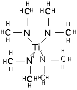
tetrakis-(dimethylamido)titanium TDMAT:
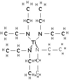
and tetrakis-(diethylamido)titanium TDEAT:
These materials are much more expensive than TiCl4. They are not unduly toxic and are stable in storage, but react slowly with moist air or rapidly with water to produce TiO2 and dimethyl or diethylamines, which have a very unpleasant odor and are moderately toxic. TDMAT is somewhat more volatile than TDEAT, but in both cases vapor pressure is low and temperatures of 80-120 °C are needed to supply vapor to the chamber. The compounds slowly decompose at these temperatures, so bubblers are inappropriate for vapor delivery, and direct liquid injection and vaporization must be employed.
The use of TDMAT alone deposits a film that has excellent conformality, but is heavily contaminated with carbon and susceptible to oxidation when exposed to air. TDMAT and TDEAT can be used in conjunction with ammonia to deposit films with much improved purity and conductivity of a few hundred microhm-cm, typically at temperatures around 350 to 400 °C and pressures of a few Torr. However, the precursors react rapidly with ammonia even at room temperature and low pressure, so it is necessary to use multi-port showerheads which prevent mixing of the gases prior to their introduction into the deposition chamber. Conformality is also degraded as more ammonia is added: there is a tradeoff between conformal deposition and purity.
One solution to this problem is to alternate deposition from TDMAT alone with a plasma treatment in N2 or NH3, which removes most of the carbon from the surface of the film and converts it to TiN. Two or three cycles of deposition and treatment suffice to produce acceptable barrier layers for electronic applications. Exposure in situ of a freshly deposited TDMAT film to silane has also been used to strip carbon and stabilize the film to atmospheric exposure, at some cost in resistivity.
Ternary TiSiN materials have been shown to be effective barriers to Cu diffusion and reaction, rivaling Ta-based materials. CVD of ternary barriers using TDEAT, NH3, and SiH4 proceeds at temperatures of 300-450 °C, producing sidewall coverage of > 80% in a 1:1 aspect ratio hole. However, the resistivity of these materials increases with increasing Si and N content, especially when N exceeds 40 at% of the material. The best compromises so far reported achieve excellent reliability in contact with copper, surviving anneals at up to 850°C without degradation, but at the expense of film resistivity of 3000 µcm. The microstructure of these materials appears to be characterized by very small Ti-rich "nanocrystals" embedded in an amorphous matrix, perhaps mostly silicon nitride; thus, they are similar to cermets, metal-ceramic composites prepared by sputtering whose resistivity is very sensitive to composition and microstructure.
Chen et. al. have reported some CVD work using TiCl4 and TiI4 for TiN deposition in contacts to silicon or silicide. No details of the deposition process were provided. Jain et. al. describe use of CVD TiN films as copper diffusion barriers. No details of the experimental method are provided. Resistivity of 200-400 microhm-cm is obtained with a tradeoff between throughput and behavior: we may tentatively infer that the process being employed is the plasma treatment of TiN from TDMAT mentioned above. They also discuss the use of nitridation of the oxide, achieving lower contact and line resistances since the area consumed by the TiN is avoided.
In 1997, Venkatesan described results using copper clad with TiN; he gave no details but it is reasonable to infer that this is CVD TiN.
Other Barrier Metals: TaN, WN, MoN
Ta-based materials make good copper barriers. Sputtering can be used to deposit them, but work has been performed on CVD of Ta and TaN using TaBr5 as a precursor. TaN films, employing NH3 as a nitrogen source, contain < 1% Br; Ta films contain about 3% Br. Excellent conformality can be obtained from thermal deposition but the nitride tends to incorporate a high-resistivity Ta3N5 phase. This undesired phase can be eliminated by using low-power PECVD with nitrogen and hydrogen instead of ammonia; however, step coverage was not reported and is often degraded in PECVD due to formation of highly reactive radicals with high sticking coefficients.
Lu et. al. describe PECVD from WF6/N2/H2 to deposit WN without gas phase reaction problems. They provide no details of the process except that temperatures from 360 to 460°C were employed.
At the 1997 International Electron Devices Meeting, Sun described the use of MoN from Mo(BuN)2(NEt2)2, but provided no experimental details.
So many references that you can see I worked on some of these films back in ancient times:
"Chemical Vapor Deposition of Titanium Nitride at Low Temperatures" S. Kurtz and R. Gordon Thin Solid Films 140 277 (1986)
"Plasma-assisted chemical vapor deposition of titanium nitride in a capacitively-coupled radio-frequency discharge" J. Laimer, H. Störi and P. Rödhammer J. Vac. Sci. Technol. A7 2952 (1989)
"The deposition rate and properties of the deposit in plasma enhanced chemical vapor deposition of TiN" D. Jang, J. Chun and J. Kim J Vac Sci Technol A7 31 (1989)
"Benefits and Limits of the Thermodynamic Approach to CVD Processes" C. Bernard and R. Madar in CVD of Refractory Metals and Ceramics Boston, Nov 29 1989, ed. Besmann and Gallois, MRS 168, p. 3
"Kinetics of Chemical Vapor Deposition of Titanium Nitride" N. Nakanishi, S. Mori and E. Kato J. Electrochem. Soc. 137 322 (1990)
"Growth and Properties of LPCVD Titanium Nitride as a Diffusion Barrier for Silicon Device Technology" A. Sherman J. Electrochem Soc. 137 1892 (1990)
"Growth Characteristics and Properties of TiN Coating by Chemical Vapor Deposition",H. Cheng, M. chiang and M. Hon, J Electrochem Soc 142 p. 1573 (1995)
"Atomic Layer Epitaxy Growth of TiN Thin Films",M. Ritala, M. Leskela, E. Rauhala and P. Haussalo,J. Electrochem Soc 142 p. 2731 (1995)
"Kinetics of the Formation of Titanium Nitride Layers by Rapid Thermal Low Pressure Chemical Vapor Deposition from TiCl4-NH3-H2",L. Imhoff, A. Bouteville, and J. Remy, J. Electrochem. Soc. 145 p. 1672 (1998)
"Silicon Dimethylamido Complexes and Ammonia as Precursors for the Atmospheric Pressure Chemical Vapor Deposition of Silicon Nitride Thin Films" R. Gordon, D. Hoffman and U. Riaz [Harvard] Chem Mater 2 481 (1991)
"Synthesis of Thin Films by Atmospheric Pressure Chemical Vapor Deposition Using Amido and Imido Titanium (IV) Compounds as Precursors" R. Fix, R. Gordon, and D. Hoffman Chemistry of Materials 2 235 (1990)
"Titanium Nitride Thin Films: Properties and APCVD Synthesis Using Organometallic Precursors" B. Fix, R. Gordon and D. Hoffman (CVD) of Refractory Metals and Ceramics, Boston, Nov. 1989 MRS Symp Proc V 168 p. 357 (1990)
"Flow Tube Kinetics of Gas Phase CVD Reactions" and "Flow Tube Kinetics of Gas Phase Chemical Vapor Deposition Reactions: TiN from Ti(NMe2)4 and NH3" Bruce Weiller and Brenda Partido, Chemistry of Materials 1994 6 p. 260
"Deposition of TiN thin films by organometallic chemical vapor deposition" thermodynamical predictions and experimental results",C. Jimenez, S. Gilles, C. Bernard and R. Madar, Surface and Coatings Technology 76-77 p. 237 (1995)
"Chemical Vapor Deposition of TiN from Tetrakis(dimethylamido)titanium and Ammonia: Kinetics and Mechanistic Studies of the Gas Phase Chemistry", B. Weiller [Aerospace], J. American Chem. Soc. 118 p. 4975 (1996)
"A Novel Process for Fabricating Conformal and Stable TiN - Based Barrier Films", J. Lu, H. Hsu, Q. Hong, G. Dixit, J. Luttmer, R. Havemann and L. Magel, J. Electrochem. Soc. 143 p. L279 (1996)
"Effect of Dimethylamine on the Chemical Vapor Deposition of TiN from Tetrakis (dimethylamido)titanium and Ammonia", B. Weiller and S. Adamson, J. Electrochem. Soc. 144 p. L40 (1997)
"The Improvement of Electrical Properties of TiN Film Deposited by MOCVD Using TDMAT", H-L Park, J-T Kim, S-B Hwang and J-C Kim p. 241 of "Advanced Metallization and Interconnect Systems for ULSI Applications in 1995", Oct. 3-5, Portland, Oregon, ed. Russell Ellwanger, Shi-Qing Wang; MRS Conference Proceedings ULSI XI (1996)
"Low Temperature and Low Pressure Process Metallorganic Chemical Vapor Deposition (MOCVD) of Superior Barrier Layers in Advanced ULSI Devices", A. Sekiguchi, H. Jimba, S. Kim, T. Yoshimura, K. Watanabe, S. Mizuno, S. Hasegawa, O. Okada, N. Takahashi and N. Hosokawa, ibid p. 355
"Resistivity Enhancement of CVD TiN with in-situ Nitrogen Plasma and its Applications in Low Resistance Multilevel Interconnects", J. Iacoponi, D. Liao, J. Tseng, M. Danek, K. Littau, D. Saigal, M. Eizenberg and R. Mosely ibid p. 375
"Low Pressure Chemical Vapor Deposition of TiN from a New Metalorganic Precursor", D.-H. Kim, J. Kim, J. Lee, J. Park and J. Kim ibid p. 381
"Electrical Characterization of MOCVD TiN for ULSI Metallization", C. Yu, L. Liu, C. Wang, B. Roberts, R. Jackson and E. McInerney ibid p. 417
"Integration of chemical vapor deposition titanium nitride for 0.25 µm contacts and vias", A. Westerheim, J. Bulger, C. Whelan, T. Sriram, L. Elliott, and J. Maziarz [DEC], J. Vac. Sci. Tech. B16 (5) 2729 (1998)
"Characterization of Ti-Si-N and W-Si-N barrier metals for Cu interconnects", T. Iijima, Y. Shimooka, and K. Suguro, in "Advanced Metallization and Interconnect Systems for ULSI Applications in 1995", Oct. 3-5, Portland, Oregon, ed. Russell Ellwanger, Shi-Qing Wang; MRS Conference Proceedings ULSI XI (1996), p. 325
"Reactively Sputtered Ti-Si-N Diffusion Barriers", X. Sun, J. Reid, E. Kolawa and M. Nicolet, ibid , p. 401
"The Diffusion Barrier Property of TiN and TaN for Cu Metallization", K-B Kim, ibid , p. 281
"Ta and Ta(N): A High Reliable Diffusion Barrier and Protection Layer for Copper Metallized Integrated Circuits", C. Wenzel, M. Stavrev, F. Rudolf, A. Preub, A. Moller, K. Drescher, ibid , p. 291
"Low Temperature, In-Situ Chemical Vapor Deposition of Tantalum and Its Nitrides for Diffusion Barrier Applications in ULSI", X. Chen, G. Peterson, T. Stark, H. Frisch, and A. Kaloyeros, VMIC 1997 p. 434
"Low Temperature Chemical Vapor Deposition of Binary Nitrides for Emerging Computer Chip Metallization", A. Kaloyeros, J. Kelsey, X. Chen, L. Xian, T. Stark, 44th National Symposium of the American Vacuum Society, San José, CA, October 20-24, 1997.
"TiCl4 and TiI4 based inorganic CVD Ti/TiN films for Gigabit DRAM contact metallization", Y.P. Chen, G. Dixit, J.P. Lu, J. Luttmer and R. Havemann, in "Advanced Metallization and Interconnect Systems for ULSI Applications in 1997", San Diego, CA, September 29 1997.
"An Ammonia-Free PECVD Process for Depositing Tungsten Nitride Films and its Application in Copper Metallization", J.P. Lu, Q.Z. Hong, W. Y. Hsu, G. Dixit, V. Cordasco, S. Russell, J. Luttmer, R. Havemann, L. Magel and H.L. Tsai, ibid.
"CVD TiN and Embedded Barriers for Copper Interconnect Technology", A. Jain, C. Simpson, T. Saaranen, R. Venkatraman, R. Bajaj, C. Dang, S. Das, J. Farkas, D. Watts, C. Capasso, J. Gelatos, R. Islam, B. Smith, T. Sparks, P. Crabtree, S. Filipiak, C. King, B. Fiordalice, H. Kawasaki, J. Klein, S. Venkatesan, E. Weitzman, ibid.
"Process Technologies for Advanced Metallization and Interconnect Systems", S. Sun, 1997 International Electron Devices Meeting, Washington, D.C., Dec. 8-10, technical digest p. 765
"A High Performance 1.8 V, 0.2 µm CMOS Technology with Copper Metallization", S. Venkatesan et. al., ibid p. 769
"Full Copper Wiring in a Sub-0.25 µm CMOS ULSI Technology", D. Edelstein et. al., ibid. p. 773
Return to Tutorial Table of Contents
Book version of the CVD Tutorial