High Density Plasma Deposition: Reactor Design
The first commercial HDP oxide deposition reactor designs were based on electron cyclotron resonance plasmas. For example, the Lam Epic reactor looked schematically something like this:
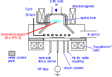
Although most modern HDP tools are based on inductive plasma generation, this reactor design illustrates many of the elements common to all HDP reactors:
- High density plasma source: in the Epic reactor, an ECR plasma was created by illuminating a magnetized region with high-power microwave radiation. At a magnetic field of about 875 Gauss, the electron Larmor frequency is equal to the microwave frequency of 2.45 GHz (another frequency used for economic reasons: it is the microwave oven frequency). At low enough pressures, electrons gain energy on each circuit around the field lines: the field allows both confinement and efficient electron heating. ECR sources can achieve densities around 1012/cm3 at pressures of a few mTorr (this is several percent ionization!).
- Big pumps: to deposit at high rates, relatively large flows of silane (and thus oxygen and argon) are required. To achieve a throughput of about 12-15 wafers per hour from a module for a deposited film 0.75 micron thick, we might require a deposition rate of about 5000 Å/minute. About 14 sccm of silane are required simply to provide enough silicon atoms to deposit this film on the wafer surface, but the film deposits everywhere in the chamber. A realistic flow might be 30 sccm of silane, with roughly twice as much oxygen and some argon: perhaps 150 sccm total flow. That may not seem like a lot, but at 5 mTorr it is a volumetric flow of 23,000 liters/minute or about 400 liters/second! The pumping capacity required to remove the gas is even larger, since the pump ports and gate valves have a finite conductance: several thousand liters per second is needed for practical reactors. Fast pumping of hydrogen is needed as well, since this gas is generated by the decomposition of the silane. The only usable approach is to employ turbomolecular pumps. Turbo pumps which can achieve these speeds are very large, very heavy, and very expensive: tens of thousands of dollars for each unit.
- Wafer RF bias: The ECR plasma has a very low plasma potential. In order to achieve significant sputtering rates at the wafer, it is necessary to apply an RF bias, which involves a separate power supply and matching network (but has the nice feature that plasma density and ion energy are then independently controllable). Several hundred volts of ion energy are required. Recall that the current density is on the order of e.g. 10 mA/cm2, for a total current of about 3 amperes to a 200 mm wafer. Typical RF bias power for a 200 mm wafer is 500-1000 Watts, almost all of which is dissipated onto the wafer surface.
- Wafer temperature control: At the low pressures of operation of HDP reactors, very little heat will be transported from the wafer by conduction or convection; recall from our discussion of showerhead heat transport that radiation will dominate at high temperature and low pressure. To remove 500 Watts from a 200 mm wafer by radiation, the wafer would need to achieve a temperature of about 500 °C, much too high for use in conjunction with Al or Cu metallization. Thus it is necessary to monitor and control the wafer temperature. The control is usually achieved by injecting a small flow of helium behind the wafer to raise the pressure to a few 10's of Torr there; however, the resulting force must be compensated to keep the wafer in position, requiring the use of mechanical clamps or an electrostatic chuck.
- Gas injection: It is necessary to put the silane into the chamber, and ideally to dispense it close to the wafer so that efficiency of utilization is improved. For total gas flows of 100-200 sccm in the typically large chambers employed in HDP, transport is dominated by diffusion. The mean free path may be as large as 1 cm, however: transport in local regions cannot be modeled accurately using continuum techniques. Thus design of the injecting apparatus is difficult, and it may also be necessary to compromise efficiency to improve uniformity.
- Chamber clean: The combination of high density plasma, low pressure, and high sputtering rates at the wafer surface means that a lot of the silicon dioxide formed ends up on the chamber walls. This buildup will spall off, creating particles, if it becomes too thick. The Lam reactor had water-cooled walls to help avoid temperature variations that would increase spalling. Nevertheless, it is also necessary to remove the deposit from the walls periodically, typically after 10-25 wafers. This may seem straightforward: there's already a high density plasma, so if one introduces some source of fluorine the oxide will etch. However, many difficulties arise. Etching SiO2 requires either copious ion bombardment or high fluxes of fluorine (i.e. high pressures, typically several Torr). High-density sources don't operate well at these pressures, and at low pressure the plasma potential is small so there's no wall bombardment. Inductive sources operated at high pressure tend to concentrate the power delivery very near the wall, which can lead to localized heating of the dielectric liner ("dome") and consequent erosion and cracking. One approach is to use a separate microwave plasma source remote from the chamber to provide fluorine for chamber cleaning.
An inductive plasma realization is shown schematically below:
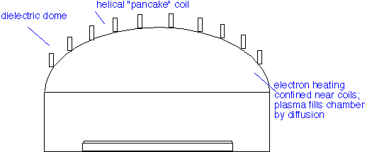
In this case, the inductive coils are distributed over the ceiling to provide improved plasma uniformity over the wafer surface, vs. a solenoidal coil. However, in both cases the actual electron heating is confined to within a skin depth of the coils; rapid diffusion at low pressure enables the plasma to fill the chamber.
Return to Tutorial Table of Contents
Book version of the CVD Tutorial