HDP Reactor Implementation Issues: Wafer Chucks and Chamber Cleaning
Too Darn Hot
Recall that in order to achieve simultaneous sputtering and deposition, it is necessary to apply RF bias power to the wafer: 500-1000 W is typical for a 200 mm wafer. This power is mostly coupled to the ions which bombard the wafer, and thus mostly dissipated at the wafer surface. As we've seen in studying heat transfer in a showerhead reactor, at the low pressures at which HDP reactors operate heat transfer from the wafer will be almost solely through radiation. Even if the chamber and chuck are cooled and absorptive, wafer temperatures exceeding 500 °C are required to radiate this heat away. Such a temperature is too high for many applications for HDP processes. [reference: "Low temperature etch chuck: Modeling and experimental results of heat transfer and wafer temperature" D. Wright, D. Hartman, U. Sridharan, M. Kent, T. Jasinski and S. Kang J. Vac. Sci. Technol. A10 1065 (1992)]
An obvious solution to this problem is to provide some gas (typically helium due to its inertness and thermal conductivity) on the back of the wafer to improve heat transfer to the chuck. A pressure of 5-10 Torr will provide significantly improved heat transfer. However, this much pressure also exerts a force much larger than the force of gravity on the wafer:
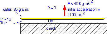
Some means of holding the wafer in place is necessary, lest it "float" like an air hockey puck, while also filling the chamber with the backside gas. Mechanical clamps have been widely used in etching, and are fairly simple to implement. However, they are sources of contamination and particles. In deposition reactions where the film will be deposited at the contact between clamp and wafer, each time the clamp is raised to release the wafer, the deposited film is shattered and particles are spewed onto the wafer edge. Finally, since mechanical clamps hold only the wafer edge, the wafers bow under the gas pressure, requiring a specially machined chuck surface for uniform heat transfer. Most commercial systems therefore employ an electrostatic chuck to clamp the wafer in place.
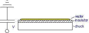
Electrostatic Chucks
The simplest electrostatic chuck consists of a conducting electrode, an insulator, and the wafer (electrically connected to the plasma) as a counter-electrode, forming a capacitor:
The energy stored in the capacitor depends on the thickness of the insulator "d".
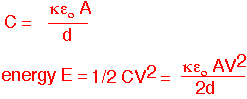
The force exerted on the plates of the capacitor can therefore be found by taking the derivative of the energy with respect to the separation. Note that the result is quadratic in the voltage and the thickness of the insulator.
Let's look at some typical numbers, using aluminum oxide as an example insulator.
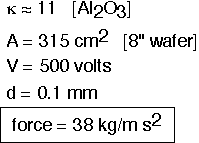
We see that typical voltages are around 500 volts to achieve a force equal to that resulting from a backside gas pressure of around 10 Torr (as calculated above).
Electrostatic Chuck Challenges
- Gas distribution: A flat chuck in contact with a flat wafer held in place by applied electrostatic forces forms an entirely too effective gas seal: the backside helium won't spread uniformly under the wafer if dispensed only in one place. It is necessary to carve channels in the chuck for the helium to travel in. The insulator thus has to be thick enough to allow the channels to be cut, but this means that the clamping force is reduced. To make up for the reduced clamping force for an ideal insulator, an electrically leaky insulator is employed: the surface of the insulator becomes charged except very near the locations of actual contact with the wafer, so that the "d" term in the force expression is just the actual separation between the wafer and the chuck surface (the "Johnson-Raybeck effect"). The leaky insulator is often prepared by adding titanium to a ceramic, but the titanium would be removed if the chuck surface were exposed to a fluorine plasma. The chuck needs to be covered by a protective wafer or blank each time the cleaning cycle is run: this adds administrative complexity and risk of destroying a very expensive chuck by procedural error.
- Unclamping: Since the plasma is the counter-electrode in a "unipolar" chuck, it is difficult to remove the wafer if the plasma is turned off, either unintentionally or because a problem is encountered elsewhere in the tool. Bipolar chucks partially solve this problem by providing two electrodes with voltage applied between them, but require more complex electrode and insulator design. In either case, the use of the Johnson-Raybeck effect means that residual charge remains on the insulator surface even when all charges are removed from the electrodes, causing the wafer to tend to stick in place. Some attention is therefore required to unclamp the wafer: one approach is to apply one or more reverse-polarity voltage steps (opposite of the clamping potential). In automated handling systems, a failure is a significant annoyance: lift pins pressing against a still-clamped wafer may cause it to shatter, necessitating that the tool be taken off line, opened, cleaned, and reconditioned before it can be returned to operation.
Note that the chuck design also has to support the uniform application of RF bias values and provide cooling to remove the considerable resulting heat. The surface must tolerate temperatures of several hundred degrees C, and ideally provide access for temperature monitoring equipment. The design of a reliable, inexpensive, serviceable chuck for HDP deposition is challenging.
[Some electrostatic chuck references:
"Manufacturing issues of electrostatic chucks" D. Wright, L. Chen, P. Federlin and K. Forbes, J. Vac. Sci. Technol. B13 1910 (1995)
Electrostatic Chuck Modeling Report SEMATECH 93061683A-ENG R. Wright & B. Lane 6/24/93
"Electrostatic Clamping Applied to Semiconductor Plasma Processing" I. Theoretical Modeling and II. Experimental Results J.-F. Daviel , L. Peccoud and F. Mondon ; J. Electrochem. Soc. 140 3245 (1993)]
Chamber Cleaning
In an HDPCVD reactor, the high plasma density combined with low pressure guarantees that the silane gas is present everywhere in the chamber, and is decomposed to silicon dioxide everywhere. In addition, about 30% of the deposited film is sputtered off of the wafer and head towards the walls. In consequence the reactor inevitably has a lot of deposition going on on all the exposed surfaces. If this unwanted deposited film should spall off as flakes, due to thermal expansion, stress, or abrasion, particles are generated that will fall onto the wafers. So periodic cleaning of the chamber walls is essential for semiconductor applications. To maximize the amount of film that can be tolerated before a chamber clean, the wall temperature is typically actively controlled. Without such control, the huge heat load encountered when the plasma is on would cause expansion of the chamber walls, stressing the film and probably leading to spalling from sharp corners and other surfaces.
Most high-density plasma sources have a plasma potential of only a few 10's of volts. In addition, many source types, such as an inductive source, require an insulating wall of e.g. ceramic material, which would tend to float to the chamber potential even if it were large. The result is that there is very little ion bombardment to assist cleaning at the walls. It is well-known in plasma etching that etching of SiO2 with typical etchants (C2F6) requires ion bombardment to proceed at a reasonable rate.
To obtain high cleaning rates in the absence of ion assistance, one is forced to use NF3 as the fluorine precursor and operate at high pressures (e.g. 1 Torr). In this regime, the generation of copious amounts of monatomic fluorine allows for a reasonably fast purely chemical removal of the silica. However, other problems arise: at high pressures, the inductive plasma is strongly confined to the region near the walls, and in fact tends to be localized near the center of the inductive coil. The resulting intense heating in that region can stress the ceramic casing and even cause cracking: a catastrophically expensive way to ensure a clean (new) chamber! Careful optimization of cleaning conditions is necessary to achieve high cleaning rates with minimal danger to the hardware.
An alternative approach is to place the plasma generation mechanism outside the chamber and use high gas flow rates to carry the reactive gases into the chamber. This method is really a downstream chemical etch in the gas phase. This is practical because of the relatively slow recombination of F atoms to make the diatomic molecule, especially at low pressures. The plumbing walls must be fabricated of some material which is passive to fluorine, so that they are not attacked and do not provide a recombination site for the reaction F + F => F2.
Return to Tutorial Table of Contents
Book version of the CVD Tutorial