Plasma Damage
This section is rather specific to the issues that arise during the fabrication of integrated circuits, particularly large complementary metal-oxide semiconductor (CMOS) circuits, with plasma processing.
Charging
Ions are constantly impinging on surfaces exposed to a plasma, giving rise to a net positive charge to the surface. In an RF-excited capacitive plasma, the sheath grows and shrinks during each RF cycle. During the brief time when the sheath voltage becomes very small, large electron currents can also flow. Typically, the sheath potential adjusts itself so that the integrated electron current balances the integrated ion current, giving no net charging of the surface.
When differences in plasma potential exist, the situation changes. The RF voltage is roughly the same throughout the chamber, so if the DC potential varies, some regions will receive no electron current at all (the plasma potential is more positive and the sheath never gets small enough for electrons to escape). The surfaces will charge up until the change in surface potential compensates for this inhomogeneity, or until lateral current flows in the substrate to correct the disparity in electron and ion currents.
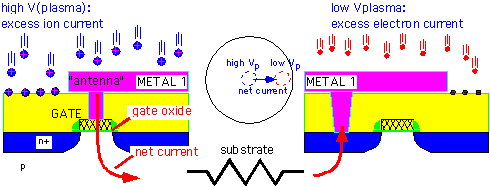
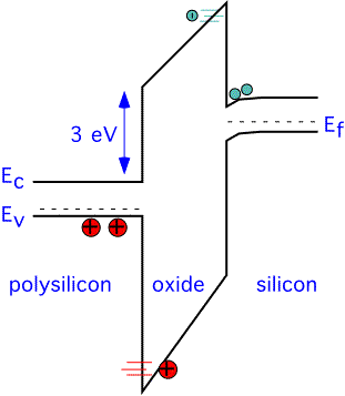
If the lateral currents flow through the oxide insulator of an MOS transistor, the reliability of the gate may be impaired, leading to reduced circuit yields or (worse) early failures once the circuits are shipped to customers. The physical origin of this effect is the formation of traps in the oxide due to energetic electrons. The band diagram below shows an MOS transistor with positive bias on the gate; electrons that can hop over or tunnel through the oxide-semiconductor barrier can travel through the oxide. Electric fields are high, and the electrons can gather energy and do damage (break bonds) as they proceed.
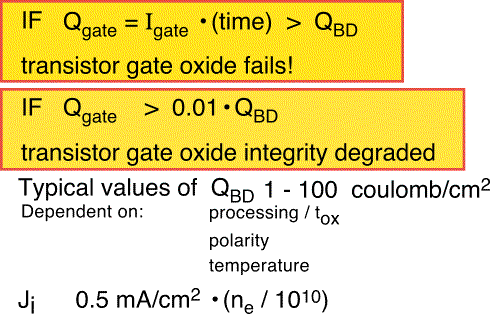
Oxide damage is generally found to be proportional to the total charge that passes through the oxide. The "breakdown charge" Qbd can be measured for a given process, and then provides the basis for useful rules of thumb about how much current can be allowed to pass through a transistor before damage occurs.
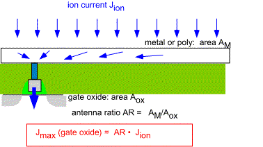
The effect can be greatly enhanced depending on the circuit design: a single transistor may be connected to a large area of exposed metal (e.g. several long wiring runs -- an "antenna") which collect a much larger total current than the transistor electrode alone would. In order to test the damage resulting from a given plasma process, one constructs test masks with varying amounts of conductive "antenna" area connected to transistors. The results are often shown as plots of damage vs. the "antenna ratio", the area of the antenna divided by that of the transistor.
Charging damage is a more serious problem in etching than in deposition, since generally the CVD film being deposited is either an insulator or a conductor: if the former, no current can flow, and in the latter case the current flows harmlessly through the deposited layer. However, charging damage has been observed in PECVD of insulating films on integrated circuit wafers. Some authors have suggested that thin insulating films remain conductive, especially under the large flux of UV light created by the plasma. The effects are exacerbated if magnetic fields are present, since as we noted the fields can cause variations in plasma potential across the reactor.
In practice, charging damage must be addressed in both process and design. Equipment and processes must be optimized to minimize damage. Circuit designers are required to avoid very large antenna ratios, either by providing diode contacts to the substrate to dissipate excess charge (these are known as antenna diodes), or introducing bridges from one metal layer to another to keep the lines short in each layer.
Charging may also result from localized variations in ion and electron flux due to topography (electron shading). Such phenomena are again more significant in plasma etching than in PECVD.
Damage from Photon and Ion Bombardment
Transistor gate oxides can also be damaged by energetic particle bombardment. The effects of ion bombardment are localized to the near-surface region, and thus generally of modest interest in PECVD, since they are ameliorated as soon as the surface is covered with a few nanometers of deposited film. [However, mechanical damage to structures can occur in high-density plasma deposition.]
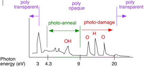
Photons with energies greater than about 10 eV can excite electrons into the conduction band of silicon dioxide from the valence band, leaving behind a trapped holes (broken bond) and probably creating damage. If the oxide is an MOS gate oxide, reliability may be impaired. Low-energy photons (4-9 eV) excite electrons into the oxide to neutralize holes created by higher-energy bombardment and can ameliorate damage. Photon energies higher than 16-20 eV can also penetrate polysilicon or metal layers, damaging the gate oxides even when they are covered by gate metal. The net result in terms of oxide damage involves a complex interaction between the spectrum of the plasma and the properties of the layers, as depicted schematically below. However, CVD oxides are also absorbers of the same photons that could damage gate oxides. Once a circuit has received a thick layer of CVD oxide dielectric, the gate oxide is well-protected from further radiation damage.
after "Effects of oxide exposure, photoresist and dopant activation on the plasma damage immunity of ultrathin oxides and oxynitrides" K. Lai, K. Kumar, A. Chou, J. Lee IEDM 1995 p. 319
---------------
Some (again old) references; note many of these are primarily relevant to etching not deposition, as this is the dominant venue for plasma damage effects:
"Plasma Charging Damage: An Overview", J. McVittie ; First International Symposium on Plasma Process-Induced Damage (P2ID), Santa Clara, CA, May 13-14, 1996, p. 7
"Monitoring Plasma-Process Induced Damage in Thin Oxide" , H. Shin and C. Hu ; IEEE Trans Semiconductor Manufacturing 6 96 (1993)
"Prediction of Plasma Charging Induced Gate Oxide Tunneling Current Antenna Dependence by Plasma Charging Probe"; S. Ma and J. McVittie [Stanford], First International Symposium on Plasma Process-Induced Damage (P2ID) Santa Clara, CA, May 13-14, 1996 p. 20
"Real Time Measurement of Transients and Electrode Edge Effects for Plasma Charging Induced Damage" S. Ma and J. McVittie, IEDM 1994 p. 463
"Charge separation in an electron cyclotron resonance plasma" M. Inoue and S. Nakamura, J. Vac. Sci. Technol. A13 327 (1995)
"Control of Plasma Damage to Gate Oxide during High Density Plasma Chemical Vapor Deposition" S. Bothra, C. Gabriel, S. Lassig and D. Pirkle, J. Electrochem. Soc. 142 L208 (1995)
"Application of Plasma Charging Probe to Production HDP CVD Tool", G. Roche and J. McVittie, First International Symposium on Plasma Process-Induced Damage, May 13-14 1996, Santa Clara, CA p. 71
"Process-Induced Charge Damage in PETEOS for Interlevel Dielectric Applications", H. Denton, G. Grynkewich, V. Ilderem, F. Lin, P. Parris, and H. Shin [Motorola], First International Symposium on Plasma Process-Induced Damage, May 13-14 1996, Santa Clara, CA p. 109
"Plasma-induced gate-oxide charging issues for sub-0.5 µm complementary metal-oxide-semiconductor technologies" A. Stamper, J. Lasky and J. Adkisson, J. Vac. Sci. Technol. A13 905 (1995)
"Reduction of the charging damage from electron shading", K. Hashimoto, Y. Hikosaka, A. Hasegawa, M. Nakamura, First International Symposium on Plasma Process-Induced Damage, May 13-14 1996, Santa Clara, CA p. 43
"Structure Dependence of Notching: Simulation of Topography Charging with Sheath Oscillation Effect", T. Kinoshita, M. Hane and J. McVittie, First International Symposium on Plasma Process-Induced Damage, May 13-14 1996, Santa Clara, CA p. 47
"A New Etching Method for Reducing the Electron Shading Damage Using ICP Etcher", S. Tabara, First International Symposium on Plasma Process-Induced Damage, May 13-14 1996, Santa Clara, CA p. 51
"Role of Temperature in Process-Induced Charging Damage in Sub-micron CMOS Transistors" T. Brozek, Y. Chan, C. Viswanathan IEDM 1995 p. 311
"Gate Material Dependence of Process Charging Damage in Thin Gate Oxide", A. Acovic, A. Ray, J. Sun, J. Herman, T. Furukawa, R. Geiger, K. Beyer, V. McGahay, S. Greco, W. Abadeer, First International Symposium on Plasma Process-Induced Damage, May 13-14 1996, Santa Clara, CA p. 160
"Mechanism of Stress-Induced Leakage Due to Plasma Charging and the Effect of Oxide Thickness", W. Abadeer, G. Huecker, A. Acovic and A. Ray, ibid p. 145
"A New Methodology for Monitoring and Comparing Edge Exposure and Plasma Charging Current Damage from Plasma Processing", S. Fonash, M. Ozaita, M. Okandan, O. Awadelkarim and Y. Chan, ibid p. 84
"A comprehensive study on radiation damage in plasma system", B. Tsui, S. Liu, G. Lin, J. Ho and C. Chang, ibid p. 148
"Fundamental Aspects of Plasma-Induced Radiation Damage of SiO2/Si : A Review", T. Mizutani, ibid p. 157
"Effects of oxide exposure, photoresist and dopant activation on the plasma damage immunity of ultrathin oxides and oxynitrides" K. Lai, K. Kumar, A. Chou, J. Lee, IEDM 1995 p. 319
Return to Tutorial Table of Contents
Book version of the CVD Tutorial