The RF in RFID: physical layer operation of passive UHF tags and readers
Daniel M. Dobkin
(revised Dec 2012)
4. RFID Tags
Passive UHF tags are typically just a bit of metal and plastic, with a single integrated circuit hidden somewhere near the middle. Sometimes they are incorporated into a human-readable label; in other cases the tag has its own adhesive and is attached directly to an object. Tags come in a variety of shapes and sizes, as shown at right.
The visible part of a tag is the antenna structure. Some tags, such as the Symbol 'X' tag shown below (the big black on the right), have two orthogonal antennas, allowing them to respond to any polarization vector in the plane of the tag; these are often known as dual dipole tags. Other tags have a single antenna, and (especially if they are long and thin) respond only to a signal polarized along their length. The ability to respond to multiple polarizations -- polarization diversity -- is quite useful in practice, as it reduces the sensitivity of the reading operation to the relative orientation of tag and reader. However, as you can see, two antennas take more space (and cost a bit more) than one antenna.
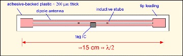
A closer look at a representative tag, an Alien Technology "I-tag", is shown below. The tag is made of a thin plastic strip known as the inlay, typically of polyethylene terapthalate (PET) or related material, often with adhesive applied on the back. The antenna structure is often made of conductive material such as copper, plated and patterned on the substrate. Printed antennas using conductive ink are also available, but their conductivity is much lower than pure metal lines, and I have observed signs of degradation in some such tags after exposure to atmosphere for 6-9 months. The antenna structure often contains some sort of metal loop, here formed by the 'inductive stubs', that acts as an inductor to resonate with the capacitance of the integrated circuit, and help match to the rest of the antenna. (Intermec tags often eschew this approach, and instead employ meandered structures to make the antenna inductive so that it matches the capacitive IC load.) The IC is often mounted on a small plastic carrier or strap, which is then bonded onto the antenna structure.
Tag antennas face several tradeoffs. As noted above, it's desirable to provide multiple antennas to allow for differing incoming polarizations, but this requires two inputs on the IC and extra space. An antenna that is 1/2 wavelength long (about 16 cm for 900-MHz operation) is resonant: that is, the local inductance and capacitance along the wire cancel, and a large current will flow in response to an impinging field, limited only by the radiation resistance. However, 16 cm is inconveniently long for many applications, so it is often of interest to make smaller structures. Various approaches can be used, such as curving or meandering the antennas, or making them broader than just a wire. In principle, an antenna properly tuned can receive the same amount of energy from an impinging field regardless of its length. However, when the tag antenna is shorter than the 'natural' resonant length, the capacitive reactance grows, and a smaller inductor value must be used to tune it to the IC; at the same time, the radiation resistance decreases. The energy stored in the reactive components increases relative to that dissipated by the radiation resistance and the load: that is, the quality factor Q of the antenna increases. Since the bandwidth of a resonator is inversely proportional to Q, smaller antennas become more narrow-band, and will have more difficulty performing across all the frequencies required for international RFID operation.
Tag integrated circuits must solve several problems: they need to convert the incident RF signal to DC power, demodulate the information in the signal, perform logic functions required by the protocol, and modulate the antenna scattering coefficient in some fashion to backscatter a signal to the reader.
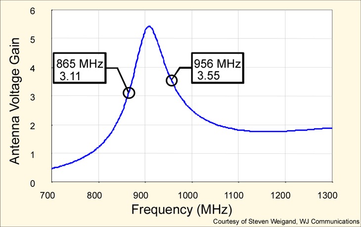
LF and HF tags can use shorted-gate MOSFETs as rectifiers, but these are generally too slow for efficient 900-MHz operation, so a Schottky or junction diode must be available in the IC process. Integrated circuits require 1-3 volts to operate. The open-circuit voltage across a short antenna is about 1/2 EincL (that is, one half of the product of the incident electric field and the length of the antenna. A radiated power of 4 W EIRP produces an electric field of about 5 V/m at 3 meters from the antenna (in the direction of the antenna beam). A 15-cm antenna will thus have an open circuit voltage of about 0.4 volts: not enough to run the IC. We need to provide some voltage multiplication. Part of the requisite increase comes from the matching circuitry, which gives a voltage gain dependent on the Q of the antenna, roughly a factor of 3-5 or so over the band. A typical simulation result is shown below. The antenna thus provides a peak voltage of around 1 to 1.2 peak volts to the IC at 3 meters, which is still a bit marginal, due to diode built-in voltages and losses.
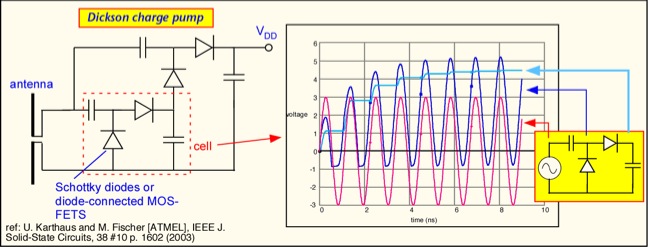
Additional voltage gain can be obtained by stacking the diode voltages; an example circuit is shown below. A time-dependent simulation of the operation of one cell, assuming ideal diodes, is shown in the graph at the right of the figure: the input RF signal (red) is offset by the shunt diode, and the resulting signal is then rectified by the series diode. By stacking a number of stages, the RF voltage can be multiplied to a higher value, though as we add more stages the parasitic capacitance of the diodes (which appear in parallel to the antenna) increases.
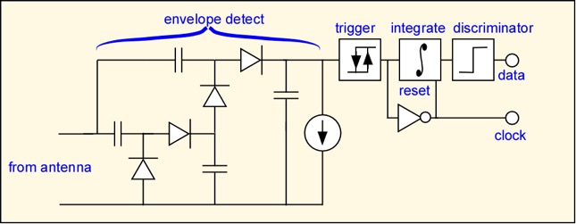
A similar charge-pump circuit, using smaller capacitors, can be used to extract a voltage proportional to the 'instantaneous' reader signal power, from which the transmitted reader symbols are obtained. Since the reader symbols are generally based on variations in the length of a pulse, a very simple demodulation scheme can be used; an example is given below, again from the work of Karthaus and Fischer. The trigger circuit is activated by a pulse edge; the integrator then integrates the output voltage until another pulse edge terminates the process, and the output is compared to the discriminator threshold to identify a binary '1' or '0'.
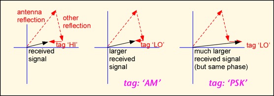
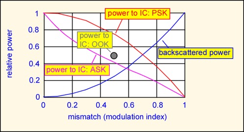
Finally, once the IC has figured out what the reader wants it to do, it needs to talk back. It does so by modifying the impedance it presents to the tag antenna. The simplest approach is to change the real impedance (e.g. by switching in an open or short circuit), but this approach has the disadvantage that when the antenna is in the alternate state, the IC can't absorb any power from the antenna. The most efficient way to modulate the impedance is to vary the reactance, e.g. by switching a capacitor into and out of the circuit. In this fashion, the phase and amplitude of the signal scattered from the antenna vary, but the IC continues to receive some energy in both states. Karthaus and Fischer denote these approaches respectively amplitude shift keying (ASK) and phase shift keying (PSK); they showed that for the same modulation index, PSK delivers about 40% more power to the IC.
Note that just because the tag is modulating the phase of its reflected signal, that does not imply that the signal the reader receives is predominantly phase-modulated. The reader signal is the sum of the tag reflection and all other reflections in the system, including that from the antenna and other obstacles in the environment; these are typically much larger than the tag reflection and with random relative phase. When the tag reflection is added to these other signals,an increase in tag reflection can result in a decrease in the received signal. A change in the phase of the tag reflection may result in a change in the amplitude of the received signal at constant phase. Examples of these cases are shown below. The reader can only hope to establish that the tag changed its state, but not how. This is why the protocols are based on detecting edges in the tag signal, irrespective of the polarity of the transitions.