Films for Self-Aligned Contacts
Summary
Many steps in IC fabrication can be "self-aligned" to previous steps if a part of the deposited insulating layer is resistant to the process that is used to etch the silicon dioxide or BPSG layers. The resulting relaxation of lithographic constraints can improve packing density and yield, at the cost of increased process complexity.
Several different stop layers have been reported in the literature: polysilicon, silicon-rich oxides and oxynitrides, and aluminum oxide. Deposition techniques include conventional PECVD, high-temperature LPCVD, and sputtering. The silicon-rich oxides or oxynitrides seem to offer the best combination of etch selectivity, process simplicity, and good electrical characteristics. However, the development of a useful self-aligned process requires metrology and process integration capabilities beyond those available to equipment manufacturers, and can only be undertaken in close partnership with an IC fab.
Film
etch selectivity
resistivity
dielectric constant
conformality
polysilicon
20:1 vs. BPSG
must be oxidized after stop
about 4 after oxidation
excellent
"SiO"
10:1 vs. SiO2
1012 ohm-cm
about 5
good?
Al2O 3
9:1 vs. SiO 2
1016 ohm-cm
about 9
poor? [sputtered]
SiON:H
7:1 vs. SiO 2
1012 ohm-cm
about 7
good?
Literature Review
Introductory Remarks
It is often necessary to achieve precise alignment between structures fabricated at different lithographic stages of IC fabrication. Consequent stringent requirements on lithographic alignment tolerance can be relaxed if the structures are "self-aligned": that is, one is forced into a specific position relative to the other for a wide range of lithographically defined positions. A familiar example is the self-aligned implant of the source and drain to a polysilicon gate, which has been used since the early 70's to achieve submicron precision in the placement of these implants independent of registration accuracy of lithography.
Multiple insulator layers which can be selectively etched provide a means of fabricating several types of structures in which lateral geometries are defined by film thicknesses, relaxing tolerances for lithographic registration. Let us consider some examples.
Contact to the source and/or drain of MOSFETs is necessary to incorporate them into functioning circuits. Contact will normally be made through an overlying layer of dielectric. If the contact holes are misaligned with respect to the gate, a short will result. The problem is depicted schematically in figure 1.
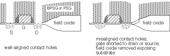
Figure 1: Misaligned S/D Contacts
In order to avoid this problem lithographically, we need to impose design rules keeping the contact holes at least a couple of alignment standard deviations from the gate edges; this forces the circuit layout to be bigger than strictly necessary.
Covering the gate with an insulating layer of SiO2 doesn't help by itself, because the oxide layer will be etched away during the contact etch: BPSG or PSG may etch somewhat faster than pure SiO2, but the gate is exposed before the contact etch is done so that high selectivity is needed. However, the combination of an oxide film on the gate and a thin "etch stop" layer will do the trick, as depicted in figure 2.
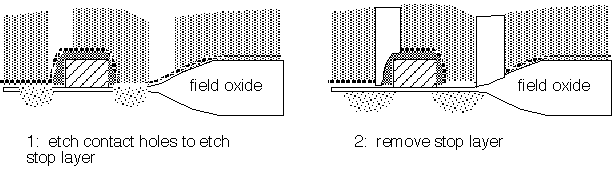
Figure 2: "Borderless" source-drain contact using etch-stop layer
The etch stop protects the gate insulation and field oxide from erosion: no contact to the gate is made despite the patterned hole overlying the gate edge. No border is required around the contact holes to the gate edge, allowing smaller source/drain regions and tighter spacings.
A highly selective etch of oxide over the stop layer is needed, since the stop layer is thin and the BPSG layer is thick. However, the removal step for the etch stop need not be very selective, since the stop layer is thin: modest removal of the underlying oxide may be tolerable.
As an alternative, the gate (or any other e.g. metal line) can be covered with an insulator other than silicon dioxide, chosen to erode slowly in an SiO2 etch process. This insulator is simply left in place, again allowing borderless contacts without creating a short.
The same approach may be used without an insulator on top of the gate to make "local interconnects" (i.e. between the source of one FET and the gate of a neighbor) without damaging the field oxide, as in figure 3. In this approach a "border" is needed between the source or drain contact and the gate line to avoid a short, but no border is needed around the contact to the subsequent gate line.
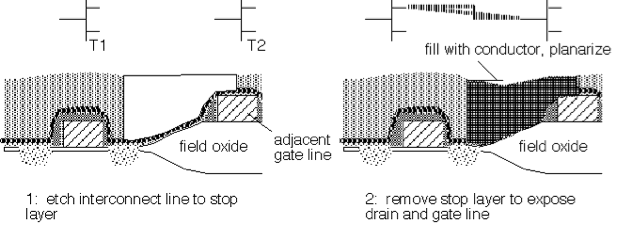
Figure 3: Self-aligned local interconnect
Note that a scheme of this nature is limited to "local" connections because the interconnect cannot cross a gate line without making a connection.
Etch stop layers can also be employed in a dual-Damascene-style process to cause the contact holes to be self-aligned to the interconnects. In this approach, trenches are formed in an insulating layer to define the interconnect lines. A second lithography then selects portions of the trenches for extra etching to create contacts to an underlying layer. Without an etch stop, the shape of these contact-to-line transitions will be influenced by the alignment accuracy of the two lithography steps, as shown in figure 4.
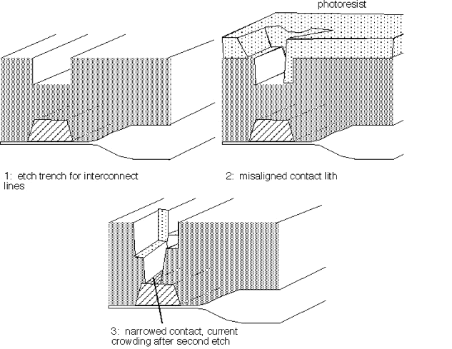
Figure 4: Dual Damascene without stop layer, misaligned contact
If an etch stop layer is placed on top of the oxide, the contact holes can be oversized perpendicular to the line without affecting the contact configuration, as depicted in figure 5.
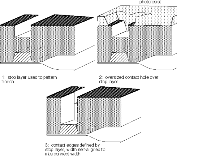
Figure 5: Dual Damascene process using stop layer, oversize contact perpendicular to interconnect
Thus there are several ways of exploiting thin layers whose etch characteristics differ from silicon dioxide or BPSG, in order to improve packing density and reduce lithographic requirements.
Let us examine how some of these schemes have been implemented in practice, and what obstacles have been encountered.
Review of the Literature
Kusters et. al. [1] implemented the borderless contact scheme depicted in figure 2, using a thin layer of polysilicon as the etch stop layer. They were able to achieve 20:1 etch selectivity of BPSG over the poly layer, so stopping on the layer was not difficult. However, the polysilicon layer is fairly conductive as deposited, and would short the circuit out if left unmodified.
To solve this problem, a layer of CVD nitride is placed under the poly layer. After etching to the polysilicon layer and then selectively removing the poly layer over the nitride, the wafers are placed in an oxidizing ambient. Oxygen is readily transported through the porous BPSG and converts the poly layer into insulating SiO2, while the underlying circuitry (and source or drain target!) is protected by the nitride layer from further oxidation. The nitride can then be removed in a moderately selective etch; since it is thin, a bit of erosion of underlying oxide or silicon is tolerable. The source and drain regions are exposed, but the gate remains protected by an insulating layer even if the contact overlaps the gate line.
In addition to the process complexity (three extra depositions and three etch steps), several problems arise in implementation of the poly etch stop [2]. The most severe is that the BPSG can flow into the contact during the oxidation step; this is most often encountered in "bordered" contacts (contacts that don't lie over gate lines). [The authors do not provide an explanation for why bordered contacts misbehave more readily; we may speculate that the higher aspect ratio of the bordered contact results in a larger effect of the BPSG surface tension, vs. the borderless contacts where the wall is partly defined by the gate line.] To solve this problem it is necessary to use high oxygen pressure oxidation at reduced temperatures; as the temperature is lowered, oxidation rate decreases less rapidly than glass viscosity increases. The authors converted from an 850°C atmospheric pressure oxidation to a 700°C high pressure step.
Oxidation also increases the volume of the polysilicon layer, as each silicon atom acquires two oxygen atoms. This causes the BPSG to swell, necessitating a second CMP step after oxidation to recover a planar surface. [What happens when you polish a surface with contact holes opened on it? Do the edges get chewed up? They don't say.] The volume expansion also sets a limit on poly thickness: at about 800 Å, the underlying nitride layer cracks during oxidation.
Fukase et. al. [3] avoided the problems of the poly etch stop layer by instead insulating the gate lines with sputtered Al2O3. Due to the low vapor pressure of aluminum fluorides, alumina is resistant to etching in fluorine plasmas: they achieved Å 9:1 selectivity using CHF3/CF4 mixtures (presumably in a conventional diode etcher). When contacts are desired, the Al2O3 layer can be removed using a BCl3 plasma.
The fundamental disadvantage of this approach is the high dielectric constant of alumina: they reported about 9.2 vs. 4 for deposited SiO2. The capacitance is still lower than that of a misaligned contact (which becomes very large just before the wires short out!), but the best-case capacitance is increased significantly.
In addition, the deposition technology seems potentially challenging. Sputtering from an alumina target requires RF rather than DC excitation and rates are typically very slow. Reactive sputtering of aluminum could be employed, but as in any reactive process the rate can be a sensitive function of conditions (depending on whether an oxide forms on the target), hardly a desirable characteristic for a manufacturing process.
Ueno et. al. [4] implemented the self-aligned contact, dual Damascene process depicted in figure 5. They initially employed polysilicon as the etch-stop layer. This appears to have worked well lithographically. However, much of their effort seems to have been devoted to developing an alternative etch stop, a silicon-rich SiOx. The justification given is process simplification; however, we may reasonably infer that the removal of the poly also caused difficulties (e.g. erosion of poly or silicon exposed at the bottom of the contact holes).
To deposit the Si-rich oxide, the authors used conventional (tube?) LPCVD with SiH4 and N2O. They don't give a temperature range, but previous work suggests that the deposition was probably around 700°C, where for SiH4-rich mixtures a substoichiometric oxide is readily produced [5]. They found that the etch selectivity (in CHF3/CO) increased with decreasing oxygen concentration in the oxide, whereas the resistivity decreased exponentially; a good compromise is about 50 at% O (essentially SiO), where 10:1 selectivity over CVD oxide is achieved with resistivities in the 1012 ohm-cm range. They filled the trench / contact structure by W CVD with RIE etchback, but one could use any other sufficiently conformal process (CVD Cu or Al) or e.g. hot Al sputtering.
White et. al. [6] used the nitride/polysilicon sandwich approach to implement a local interconnect scheme like the one depicted in figure 3 above. Just as in the work of Kusters et. al. [1], it is necessary to oxidize the polysilicon after using it to stop the contact etch. However, these authors use CMP rather than glass flow for planarization, so they employ 4wt% PSG as an insulating layer, eliminating problems with glass flow into contact holes. However, they still employ a high-pressure oxidation to reduce the thermal budget of the process. The complexity of the tradeoffs in this process is suggested by the fact that even the optimized process reported results in occasional residual poly at the bottom corner of the spacer oxide. The poly layer must be thin enough to completely oxidize but thick enough to stop the etch; selective removal of the poly must leave the nitride layer intact to avoid oxidation of the underlying gate or diffusion, which would prevent contact formation. They achieve a 4:1 selectivity of nitride to oxide, which gives them a "2X process window" (i.e., 100% overetch is allowed?).
As noted above, this type of scheme is inherently local: one cannot cross a gate line without making contact. Therefore, it is necessary to "stack" contacts to the next layer in order to allow line crossings without sacrificing feature density. These authors employ CVD tungsten and CMP for both local interconnect and stacked contact layers.
Subsequent publications confirm that improvements in etching technology are simplifying the requirements for etch stop layers. Park et. al. [9] substitute silicon nitride for silicon dioxide as the gate spacer material. Modern high-density etching using an ICP (inductively coupled plasma) source apparently achieves sufficient selectivity of TEOS/O3 ILD layer over the spacer to allow selective contacts, without requiring doping in the oxide.
Ogawa et. al. [11] exploit ECR as a high-density plasma source to obtain self-aligned contacts with an oxide/nitride etch stop layer. Here they use an "isotropic" (low bias?) mode to etch BPSG selectively to high-temperature (TEOS) oxide in SF6. A second method purposely undercuts a poly etch stop layer and then flows BPSG on top of it to seal the edges, avoiding the need for a re-oxidation step.
A quite different approach is taken by Hada et. al. [10]: they have developed a technology that not only grows Si selectively onto exposed source/drain contact regions, but that grows "anisotropically" (i.e. vertical growth rate >> lateral growth rate), enabling them to raise the Si height without encroachment onto the field oxide. They didn't describe a complete process, but we can infer that ILD deposition followed by CMP could be used to selectively expose the Si plugs, allowing low-aspect-ratio, self-aligned contacts for the capacitor level without the use of selective etching. This represents a competing approach to the standard etch-stop layer method.
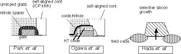
Figure 6: Alternative Etch Stop Approaches
Features of an Etch Stop Layer
We can conclude from the work described above that the ability to include an etch stop layer in a dielectric sandwich enables several methods of reducing process sensitivity to lithographic alignment. The desirable properties of such a stop layer are:
- high etch selectivity to silicon dioxide
- high electrical resistivity and breakdown voltage
- low dielectric constant
- easily etched in a commonly-available process chemistry
as well as the usual requirements for a deposited film (ease of deposition, control of stress and conformality, stability in ambient conditions).
In table I we compare the candidates discussed above. For comparison we have added plasma nitride etching results from Ueno et. al. [7] with resistivities for silicon-rich nitrides estimated from the results of Bertran et. al. [8].
Table I: Candidates
Film
etch selectivity
resistivity
dielectric constant
conformality
polysilicon
20:1 vs. BPSG
must be oxidized after stop
about 4 after oxidation
excellent
"SiO"
10:1 vs. SiO2
1012 ohm-cm
about 5*
good?
Al2O 3
9:1 vs. SiO 2
1016 ohm-cm
about 9
poor? [sputtered]
SiON:H
7:1 vs. SiO 2
1012 ohm-cm
about 7
good?
We can conclude that high-temperature CVD of silicon-rich oxides, or PECVD of nitrides, both promise stop layers with good electrical properties, adequate selectivity, and simple process integration. Polysilicon provides excellent selectivity but requires complex process integration compromises due to the necessity of post-etch oxidation. Alumina is a less familiar material handicapped with a high dielectric constant and questions about the practicality of sputtered deposition (though it seems likely that a useful thermal or plasma CVD process could be developed for this film).
Metrology
The quantities of interest for most of these applications are the film etch rates and topographic structure before and after etching. Selectivity is usually measured on blanket-coated substrates using standard thickness measurements: e.g. reflectometry (Prometrix, Nanospec, Tyger), ellipsometry, etc. for transparent films, profilometry (Alphastep) for absorbing films. Conformality and patterned shapes are characterized with cross-sectional SEM and sometimes additional TEM work.
Composition of silicon-rich films can be characterized in various ways. Refractive index is convenient but ambiguous: high refractive indices can result from either nitrogen or silicon incorporation. Auger analysis is acceptable if charging artifacts are avoided. FTIR will reveal Si-H bonds which frequency accompany Si-rich stoichiometry but is not very useful for quantifying the elemental composition. X-ray analysis is generally not very helpful for O, N and H. SIMS can be used but is probably unnecessary.
References
- "A Self-aligned Contact Process with Improved Surface Planarization", K. Kusters, W. Sesselmann, H. Melzner and B. Friesel [Siemens], Journal de Physique Colloque C4 supplement #9, volume 49 (Sept. 1988)
- "Integration of BPSG in a 0.25 µm DRAM Process", J. Gambino, M. Jaso, H. Aochi, Y. Tsunashima, M. Peschke and G. Bronner [IBM/ Toshiba / Siemens] [source unknown]
- "A Margin-Free Contact Process Using an Al2O3 Etch-Stop Layer for High Density Devices", T. Fukase, H. Hada, H. Aoki and T. Kunio [NEC], IEDM 1992 p. 837
- "A quarter-micron planarized interconnection technology with self-aligned plug", K. Ueno, K. Ohto, K. Tsunenari, K. Kajiyana, K. Kikuta and T. Kukkawa [NEC], IEDM 1992 p. 305
- "Characterization of Oxide Grown at High Temperatures and Low Pressure from Silane/Nitrous Oxide Reaction", A. Learn and R. Jackson, J Electrochem Soc 132 2975 (1985)
- "Damascene Stud Local Interconnect in CMOS Technology", F. White, W. Hill, E. Eslinger, E. Payne, W. Cote, B. Chen, K. Johnson [IBM], IEDM 1992 p. 301
- "Reactive ion etching of silicon oxynitride formed by plasma-enhanced chemical vapor deposition", K. Ueno, T. Kikkawa and K. Tokashiki, J. Vac. Sci. Technol. B13 1447 (1995)
- "Optical and Electrical Properties of a-SixNy:H Films Prepared by RF Plasma Using N2+SiH4 Gas Mixtures", E. Bertran, J. Lopez-Villegas, J. Andujar, J. Campmany, A. Canillas and J. Morante, J. Non-Cryst. Solids 137/138 895 (1991)
- "Isolation Merged Bit Line Cell (IMBC) for 1 GB DRAM and Beyond", J. Park, J. Lee, B. Hwang, S. Jo, B. Kim, S. Jang, S. Kwon, D. Kim, J. Kim, K. Kim, J. Park and J. Lee [Samsung], IEDM 1995 p. 911
- "A Self-Aligned Contact Technology Using Anisotropical [sic] Selective Epitaxial Silicon for Giga-Bit DRAMs", H. Hada, T. Tatsumi, K. Miyanaga, S. Iwao, H. Mori and K. Koyama [NEC], IEDM 1995 p. 665
- "Method for Fabricating a Semiconductor Integrated Circuit Device Including the Self-Aligned Formation of a Contact Window", H. Ogawa, Y. Naito, M. Fukumoto, assigned to Matsushita Electric, US Patent 5,275,972
Selected Shorts Table of Contents